

Global Electron Beam Lithography System (EBL) Market Set to Expand at 9.38% CAGR During 2026–2032
Electron Beam Lithography System (EBL) Market
Global Electron Beam Lithography System market is forecast to reach US$3.07 billion by 2032, driven by multi-beam, photomask and Asia-Pacific demand.
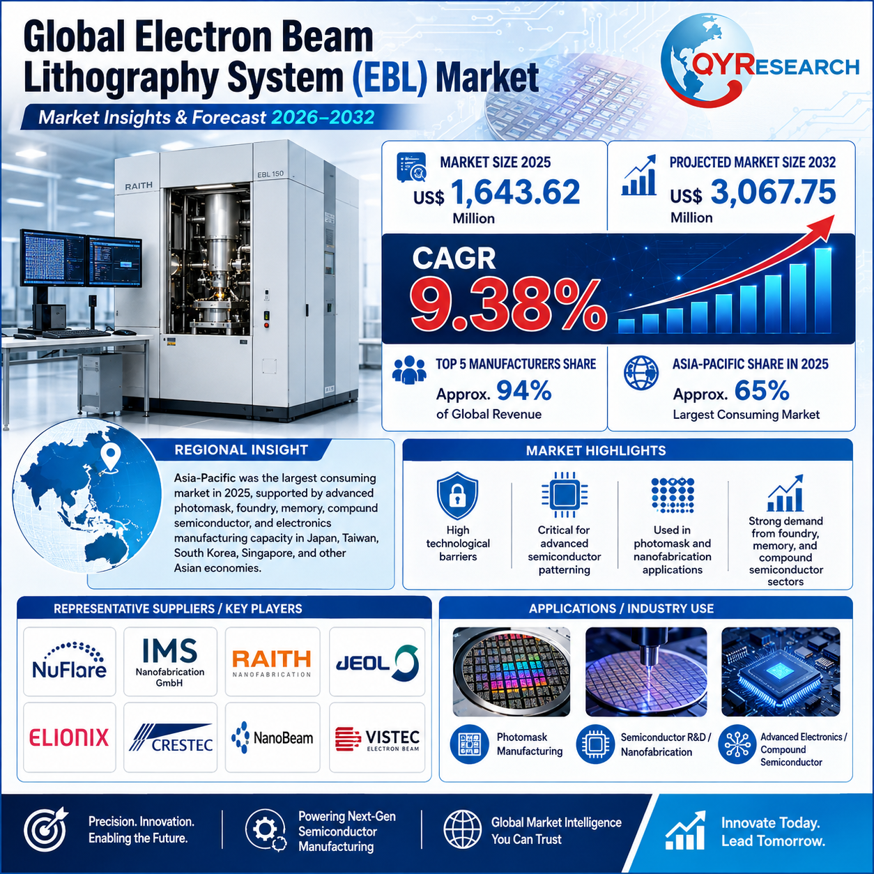
PUNE, MAHARASHTRA, INDIA, August 17, 2026 /EINPresswire.com/ -- PUNE, Maharashtra, India — August 17, 2026 — The global Electron Beam Lithography System (EBL) market is entering a new phase of technology-led expansion as advanced semiconductor manufacturing, photomask production, compound semiconductors, photonics, quantum-device research, and nanoscale fabrication create demand for higher-resolution and higher-throughput patterning systems. The market was valued at approximately US$1,643.62 million in 2025 and is forecast to reach US$3,067.75 million by 2032, representing a 9.38% CAGR during 2026–2032.Asia-Pacific remains the center of market activity, accounting for approximately 65% of global EBL revenue in 2025, reflecting the region's concentration of semiconductor foundries, memory manufacturers, photomask operations, electronics production, and advanced fabrication infrastructure.
The competitive environment is equally notable: the supplied market analysis indicates that the five largest manufacturers collectively represented roughly 94% of global revenue in 2025, underscoring the demanding engineering, precision-control, electron-optics, software, service, and intellectual-property requirements needed to compete at scale.
Download Exclusive Research Report PDF Sample: (Including Full TOC, List of Tables & Figures, Chart) @ https://www.qyresearch.in/request-sample/machinery-equipment-global-electron-beam-lithography-system-ebl-market-share-and-ranking-overall-sales-and-demand-forecast-2026-2032
Market Overview
Electron beam lithography is a precision nanofabrication technology that directs a focused electron beam onto an electron-sensitive material to create extremely small patterns. Unlike conventional optical lithography, EBL can be used for direct writing and specialized mask fabrication, making it particularly important where nanoscale pattern control, positioning accuracy, custom geometries, and research flexibility matter more than mass-production exposure speed. NIST describes electron-beam lithography as a technology capable of fine control over nanostructures used across diverse device platforms, while commercial suppliers increasingly position EBL for semiconductors, photonics, quantum technologies, compound semiconductors, and advanced research.
The US$1.64 billion-to-US$3.07 billion market expansion expected between 2025 and 2032 indicates that EBL is moving beyond a narrowly defined research-equipment category. Its addressable opportunity increasingly includes industrial photomask writing, direct-write production, advanced device prototyping, optical and photonic structures, nanoimprint master fabrication, and high-value semiconductor applications.
This transformation is occurring alongside a broader semiconductor equipment investment cycle. Worldwide semiconductor manufacturing equipment sales reached US$135.1 billion in 2025, up 15% year over year, according to SEMI. In July 2026, SEMI projected wafer-fab-equipment sales of US$143.9 billion for 2026, with continued increases expected through 2028 as manufacturers invest in advanced logic, AI computing, high-bandwidth memory, and technology migrations. These broader capital-spending conditions provide an important demand backdrop for specialized EBL equipment.
For investors and manufacturers, the important point is that the 2026–2032 EBL opportunity is not based on semiconductor unit growth alone. It is increasingly shaped by pattern complexity, photomask requirements, device diversity, resolution, overlay performance, throughput, automation, and data-processing capability.
Market Key Drivers and Dynamics
One of the strongest drivers for the Electron Beam Lithography System market is the continued scaling and increasing complexity of semiconductor manufacturing. Advanced devices require increasingly precise pattern generation, while sophisticated photomasks remain essential for modern lithographic workflows. NuFlare, for example, markets its MBM-2000 series of multi-electron-beam mask writers for advanced-node photomask production, with the MBM-2000 designed for 3 nm-node rules and the MBM-2000PLUS targeting 3 nm-plus requirements.
Multi-beam architecture is becoming especially important because the industry needs to reconcile nanoscale precision with practical writing throughput. IMS Nanofabrication identifies multi-beam mask writers as key tools for integrated-circuit production and describes itself as a commercial supplier of multi-beam systems to leading chip manufacturers. The transition from sequential beam exposure toward highly parallel writing approaches is therefore expected to be an important competitive theme through 2032.
A second driver is the widening range of nontraditional semiconductor applications. JEOL identifies EBL use cases that include photonic crystals, optical waveguides, microlens structures, MEMS, nanoimprint molds, two-dimensional materials, and quantum devices. Raith similarly positions electron-beam lithography across semiconductors, optoelectronics, and quantum technologies. These applications can broaden equipment demand beyond large semiconductor production sites into universities, national laboratories, specialist foundries, photonics companies, and emerging technology manufacturers.
Throughput remains one of the industry's defining challenges. As feature density grows, simply improving resolution is insufficient; customers increasingly require faster stages, higher beam currents, sophisticated exposure strategies, automation, improved pattern-data processing, and stable long-duration operation. Elionix's ELS-BODEN Σ, for example, uses a 400 MHz scan clock and high-speed stage architecture aimed at raising manufacturing throughput.
Market growth nevertheless faces barriers. Premium EBL systems demand substantial capital expenditure, specialized facilities, highly trained personnel, precision environmental control, and long customer qualification cycles. Semiconductor-equipment trade restrictions and export-control policies can also affect where advanced manufacturing technologies are sold, serviced, or deployed, adding geopolitical uncertainty to long-term equipment planning.
Regional Insights
Asia-Pacific is expected to remain the strategic center of the global Electron Beam Lithography System market through 2032. The region accounted for approximately 65% of EBL revenue in 2025, led by semiconductor and electronics ecosystems in Japan, China, Taiwan, South Korea, Singapore, and other Asia-Pacific manufacturing hubs.
The broader semiconductor-equipment data reinforces this position. China, Taiwan, and South Korea together accounted for approximately 79% of worldwide semiconductor equipment spending in 2025. Taiwan's equipment spending increased sharply to US$31.5 billion, while South Korea reached US$25.8 billion amid strong HBM and DRAM investment; Japan also recorded semiconductor-equipment spending growth during the year.
For the Japan Electron Beam Lithography market, the presence of established suppliers such as NuFlare, JEOL, Elionix, and Crestec strengthens the domestic technology ecosystem. Japan's longstanding role in semiconductor materials, photomasks, precision instrumentation, and electron optics gives the country relevance both as a supplier base and as an EBL consumption market. NuFlare's advanced mask-writer roadmap and JEOL's expanding direct-write portfolio illustrate this continued technology depth.
Taiwan and South Korea represent important regional opportunities due to their advanced foundry, logic, memory, AI accelerator, HBM, and semiconductor manufacturing investments. China's EBL market also carries significant long-term demand potential because of continuing investment in semiconductor capacity, although advanced-equipment trade restrictions can influence sourcing options and competitive positioning. SEMI reported China at US$49.3 billion of semiconductor equipment spending in 2025.
North America remains particularly relevant to advanced semiconductor R&D, nanotechnology, quantum research, photonics, national laboratories, universities, and specialized production. Meanwhile, Europe's EBL ecosystem benefits from companies such as IMS Nanofabrication in Austria and Raith and Vistec in Germany. Vistec's portfolio includes 200 mm and 300 mm variable-shaped-beam platforms, while European photomask operations have also been investing in modern multi-beam capabilities.
Market Segmentation
By technology type, the global Electron Beam Lithography System market is divided into Gaussian Beam EBL Systems, Shaped Beam EBL Systems, and Multi-Beam EBL Systems. Each addresses a different balance of flexibility, writing speed, resolution, substrate size, production economics, and intended application.
Gaussian beam EBL systems remain highly relevant for direct writing, advanced R&D, photonics, compound semiconductor devices, quantum structures, and applications where extremely fine, flexible patterns are essential. JEOL's JBX-8100FS, for example, uses Gaussian beam optics for direct writing, while its newer JBX-A9 supports wafers up to 300 mm and targets high-precision, high-throughput direct-write applications.
Shaped beam EBL systems are designed to improve writing efficiency by exposing variable rectangular or other shaped areas rather than relying entirely on single-spot scanning. Vistec specializes in variable-shaped-beam technology and supplies systems for industrial and advanced research applications, including compound semiconductor manufacturing, direct-write mask making, photonics, and emerging nanofabrication markets.
Multi-beam EBL systems represent one of the most strategically important areas for the forecast period. By writing with many beams simultaneously, the architecture addresses the industry's persistent throughput challenge and is particularly significant in sophisticated photomask manufacturing. IMS and NuFlare are visible participants in this technology transition.
By application, the market is categorized into Academic Field, Industrial Field, and Others. Academic demand is supported by university cleanrooms, nanotechnology facilities, physics laboratories, quantum-device programs, and materials research. Industrial demand encompasses semiconductor manufacturing, photomasks, compound semiconductors, photonics, optical communications, nanoimprint masters, and specialized device production.
Competitive Landscape
The competitive structure of the Electron Beam Lithography System industry remains unusually concentrated. Representative companies identified in the 2026 market analysis include IMS Nanofabrication, NuFlare Technology, Raith, JEOL, Elionix, Vistec Electron Beam, Crestec, and NanoBeam. The supplied research dataset estimates that the five leading manufacturers generated approximately 94% of worldwide revenue in 2025, illustrating the significant entry barriers surrounding electron optics, beam control, mechanical accuracy, pattern-processing software, process expertise, system integration, field service, and long-term customer qualification.
Competition is increasingly moving beyond a simple comparison of minimum feature size. Buyers are evaluating writing throughput, placement accuracy, overlay, stitching performance, automation, usable wafer size, uptime, stage performance, exposure software, data handling, environmental stability, power consumption, and lifetime operating cost. JEOL's JBX-A9, for example, combines 300 mm wafer capability with lower power requirements and a smaller footprint than its predecessor architecture, illustrating the industry's growing focus on productivity and facility efficiency alongside precision.
Raith competes across research and industrial nanofabrication with platforms such as EBPG, VOYAGER, Pioneer, E-LINE, and Raith150, while Elionix offers multiple acceleration-voltage configurations spanning research and lower-volume production requirements. Vistec focuses on variable-shaped-beam systems, while NanoBeam manufactures dedicated high-resolution EBL platforms.
For new entrants, this concentration creates both a challenge and an opportunity. Competing head-to-head in flagship high-end systems requires substantial expertise and capital, but specialized opportunities may emerge around workflow software, automation, process optimization, service, application-specific configurations, resist processes, metrology integration, and complementary nanofabrication infrastructure.
Market Trends, Opportunities
The most important trend through 2032 will be the effort to achieve high resolution and high throughput simultaneously. As pattern complexity increases, multi-beam exposure, faster pattern-data preparation, advanced correction algorithms, automated wafer handling, improved stage motion, and more integrated process control are expected to gain strategic importance. Current product development from IMS, NuFlare, JEOL, Elionix, Raith, and Vistec already reflects this direction.
Another trend is the movement of EBL into a broader range of commercial nanotechnology markets. Photonics, quantum computing, compound semiconductors, optical communications, MEMS, metamaterials, nanoimprint lithography, and advanced sensors require highly specialized structures that can favor direct-write electron-beam processes during research, prototyping, and selected production stages.
Questions Answered included in the Report:
(1) What is the expected size of the global Electron Beam Lithography System market by 2032?
(2) Which region offers the strongest EBL opportunity?
(3) Which technology could reshape competition most significantly?
(4) What should investors, researchers, and manufacturers monitor between 2026 and 2032?
The Global Electron Beam Lithography System (EBL) Market outlook for 2026–2032 therefore points to a specialized but increasingly strategic equipment category. With the market projected to approach US$3.1 billion by 2032, competitive advantage is likely to belong to suppliers that can combine nanoscale precision with higher throughput, dependable automation, powerful data processing, large-substrate capability, service infrastructure, and application-specific expertise. For investors, researchers, photomask producers, semiconductor manufacturers, and nanotechnology companies, EBL is becoming an increasingly important intersection of advanced manufacturing, photonics, semiconductor scaling, and next-generation device innovation.
For Further insights and Detailed Reports, Visit: https://www.qyresearch.in/report-details/0578213/Global-Electron-Beam-Lithography-System-(EBL)-Market
About QYResearch
QYResearch founded in California, USA in 2007. It is a leading global market research and consulting company. With over 19 years’ experience and professional research team in various cities over the world QY Research focuses on management consulting, database and seminar services, IPO consulting (data is widely cited in prospectuses, annual reports and presentations), industry chain research and customized research to help our clients in providing non-linear revenue model and make them successful. We are globally recognized for our expansive portfolio of services, good corporate citizenship, and our strong commitment to sustainability. Up to now, we have cooperated with more than 70,000 clients across five continents. Let’s work closely with you and build a bold and better future.
Contact US
Ankit Jain - Director, Global Digital Marketing
QY Research, INC.
India Office -
315Work Avenue, Raheja Woods, Kalyani Nagar,
Pune, Maharashtra 411006, India
Web – https://www.qyresearch.in
Email- ankit@qyresearch.com
Ankit Jain
QY Research India
+ +91 8149736330
ankit@qyresearch.com
Legal Disclaimer:
EIN Presswire provides this news content "as is" without warranty of any kind. We do not accept any responsibility or liability for the accuracy, content, images, videos, licenses, completeness, legality, or reliability of the information contained in this article. If you have any complaints or copyright issues related to this article, kindly contact the author above.
